

SYNTHESIZING AN EXCELLENT LITERATURE REVIEW
August 2, 2021
Ace Your Ph.D. With Ease: Manage Stress For A Smooth Sail
August 9, 2021Quantum dots for optoelectronic devices
Introduction
Nanometre-scale semiconductor chips have been imagined as next-generation technology with high functionality and convergence. Quantum dots, also known as artificial atoms, have special properties owing to their quantum confinement in all three dimensions. Quantum dots have a lot of interest in optoelectronic systems because of their special properties. Many attempts have been made worldwide to improve the efficiency and functionality of these promising nanomaterials for next-generation optoelectronic devices like lasers, photodetectors, amplifiers, and solar cells. Quantum dot devices with outstanding performance surpassing prior devices have been demonstrated by producing optoelectronic devices based on quantum dots over the last two decades. The progress in quantum dots for optoelectronic devices has been described in this article over the last few years.
Research advancements in quantum dots
For decades, self-assembled nanostructures have been a topic of considerable concern and significance. By shrinking the dimensions of a semiconductor to a nanoscale, certain special properties, such as quantum effects, can be obtained. The electrical and optical properties of nanometre-sized semiconductors can be manipulated by manipulating their morphology, thanks to the quantum scale effect. Semiconductor quantum dots (QDs), similar to electrons, are a fascinating nanoscale structure of confined carriers in all dimensions. Compared to conventional bulk semiconductors, 0D semiconductor nanostructures are more tuneable and sensitive to external parameters. Furthermore, since QDs are zero-dimensional, they have distinct energy levels and a density of states that can be reduced to a set of delta functions.
Low-dimensional semiconductors have gained a lot of interest because of their fundamental advantages. This can be observed in the 1970s; Dingle and Henry discovered quantum-organized semiconductor lasers could achieve wavelength tunability and threshold reduction [1], which was later theoretically demonstrated in the 1980s by Asada et al. and Arakawa et al. [2]. Since there was no feasible fabrication technique for QDs for several years after these pioneering works, the efforts dedicated to QDs and their implementations in devices were only experimental research. Due to major advancements in epitaxial development techniques, self-assembled QDs were impossible to make until the early 1990s. After self-assembled QDs were successfully fabricated, laser diodes based on QDs running at 77 K were quickly developed. Following the good demonstration of self-assembled QDs and the first QD laser, a worldwide initiative was launched to improve QD growth control and manufacture high-performance laser chips. The majority of research on self-assembled QDs focuses on material structures with mismatched lattices, such as In(Ga)As/GaAs [3] and InAs/InP [4]. Thermodynamic arguments are often used to explain heteroepitaxial growth modes in thin films.
The improvement made in QD self-assembly was quickly rewarded. Quantum dot infrared photodetectors (QDIPs) [3], quantum dot solar cells (QDSCs) [5], quantum dot superluminescent diodes (QDSLDs) [6], and quantum dot amplifiers [7] have all been documented, in addition to lasers. The invention of mid-wavelength and long-wavelength infrared photodetectors [5] was prompted by inter-subband absorption in QDs in the late 1990s. Several groups published QDSCs, quantum dot amplifiers, and QDSLDs in the 2000s. The work on optimizing material growth and product architecture is still going on to deliver on the promise of high-performance QD optoelectronic products. As seen in figure 1, the threshold current density of QD lasers has recently reached the highest value for QW lasers produced for many decades.
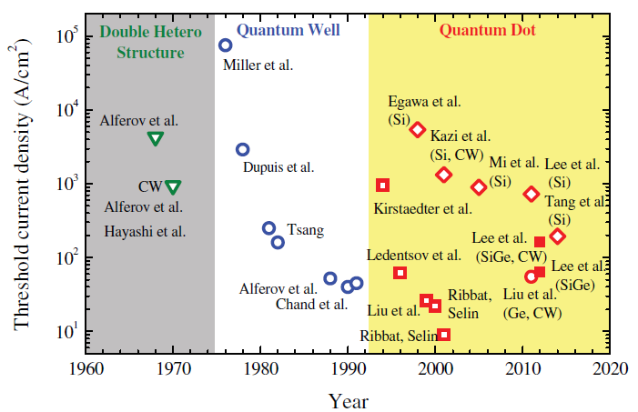
Figure 1. The record threshold current densities at the time of publication can be seen in the historical history of heterostructure lasers [8].
Future Scope
Since these nanostructures were first grown and categorized, self-organized quantum dot optoelectronic devices have come a long way. Quantum dot lasers are now on par with quantum well lasers in terms of efficiency. Inter-sublevel instruments, which can be used as light sources and detectors and can operate in a surface-normal mode, have increased efficiency and special properties. Quantum dot optoelectronic sensors are expected to play a major role in upcoming systems. High-performance QDIPs are also possible thanks to the intensive research activities in QDs. QDIPs have basic benefits over Quantum Well Infrared Photodetector (QWIP) in that they can run at higher temperatures and have lower dark current. QDIPs are now outperforming QWIPs in terms of efficiency. QDIPs have outperformed QWIPs in terms of operating temperature. Several issues remain, such as inadequate quantum performance, and QDIP architecture and fabrication must be enhanced to realize their potential in third-generation infrared sensing. QDIPs with efficiency comparable to existing state-of-the-art technologies such as QWIPs and HgCdTe photodetector may be used in the coming years. Due to various fundamental shortcomings, such as QDs’ slow absorption and the extreme thermal connection between the intermediate and conduction bands, QDSCs are the least evolved of the various forms of QD optoelectronic systems. Further advances in device physics, design, growth, and characterization of QDSCs would be needed to achieve high conversion efficiency beyond the record value of GaAs single-junction solar cells.
Reference
[1] Dingle R and Henry C H 1976 Patent Number US3982207 A
[2] Asada M, Miyamoto Y and Suematsu Y 1986 IEEE J. Quantum Electron. 22 1915–21.
[3] Hamsavahini Rajanna, Kaustab Ghosh, Minimization of bandstructure dependent dark current in InAs/GaAs quantum dot photodetectors, Superlattices and Microstructures, 2021, 106919,
[4] Mohamed Helmi Hadj Alouane, Olfa Nasr, Hammadi Khmissi, Bouraoui Ilahi, Gilles Patriarche, Mohamad M. Ahmad, Michel Gendry, Catherine Bru-Chevallier, Nicolas Chauvin, Temperature dependence of optical properties of InAs/InP quantum rod-nanowires grown on Si substrate, Journal of Luminescence, Volume 231, 2021, 117814,
[5] Zhang, L., Kang, C., Zhang, G., Pan, Z., Huang, Z., Xu, S., Rao, H., Liu, H., Wu, S., Wu, X., Li, X., Zhu, Z., Zhong, X., Jen, A. K.‐Y., All‐Inorganic CsPbI3 Quantum Dot Solar Cells with Efficiency over 16% by Defect Control.Adv. Funct. Mater. 2021, 31, 2005930.
[6] Ya-Qi Qiu, Zun-Ren Lv, Hong Wang, Hao-Miao Wang, Xiao-Guang Yang, and Tao Yang, “Improved linewidth enhancement factor of 1.3-µm InAs/GaAs quantum dot lasers by direct Si doping”, AIP Advances 11, 055002 (2021)
[7] Mukherjee, K. A terabit-per-second all-optical four-bit digital-to-analog converter using quantum-dot semiconductor optical amplifiers. J Comput Electron (2021).
[8] Jiang Wu et al. 2015 J. Phys. D: Appl. Phys. 48 363001.